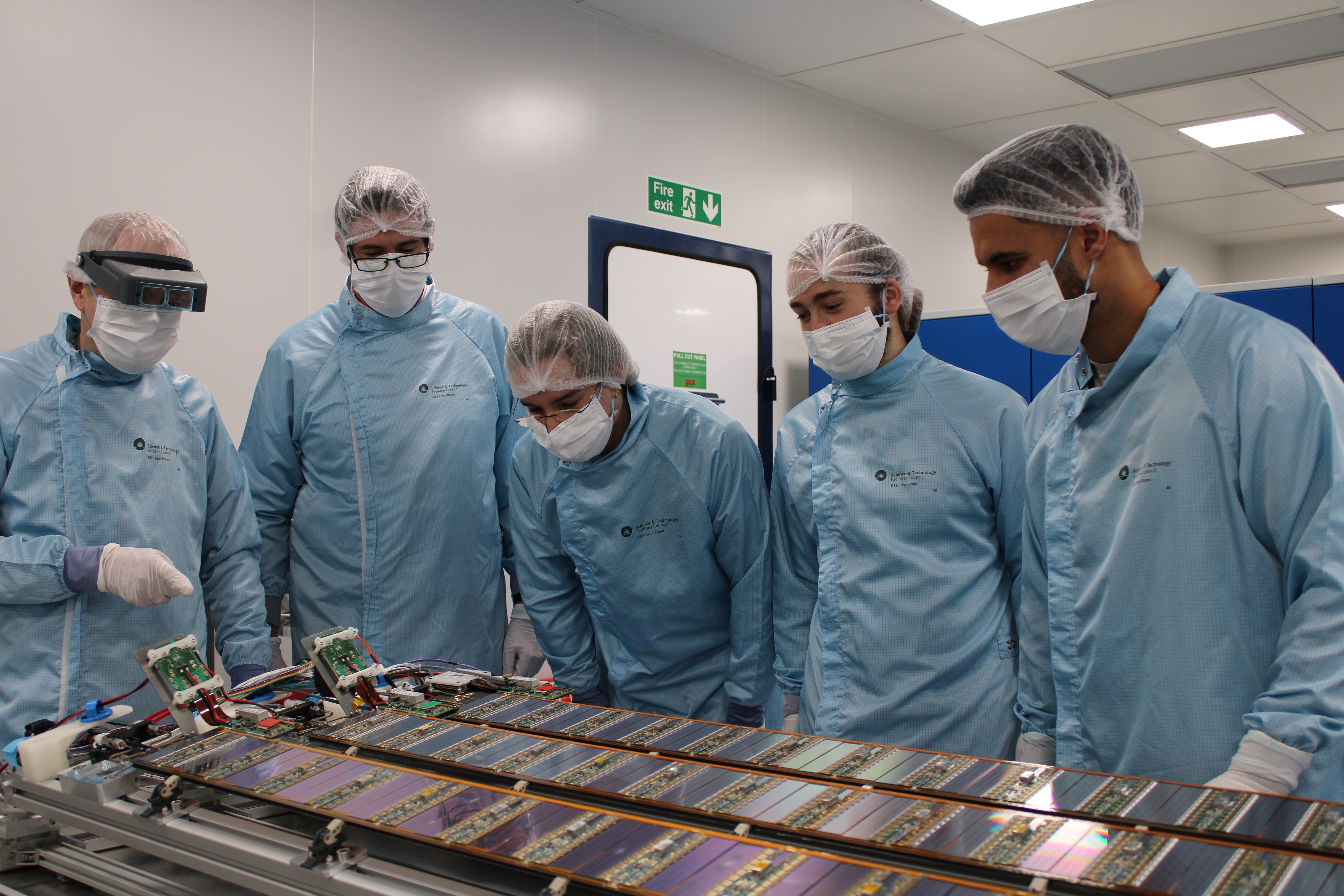
The Science and Technology Facilities Council provide electronics assembly and packaging services for electronic systems with a primary focus on the assembly and packaging of semiconductor devices such as readout ASICs combined with a variety of radiation detectors.
Common design challenges include the need to be able to pass specific electromagnetic radiation and control signals into a sensor and pass the response out for further processing. These responses can be a mix of digital and analogue electronic signals, the latter often digitised and converted to optical signals as soon as possible.
To meet the need for heterogenous integration in such systems the Interconnect team maintain a range of capabilities appropriate for small to medium-volume production including:
- Design for appropriate packaging material, such as circuit boards
- Forming arrays of micro bumps, to prepare devices for flip chip bonding
- Complete flip-chip bonding of large (or small) area arrays
- Perform die-attach, down to micron-level accuracy
- Make point-to-point connections by wire bonding
- Carry out inspection and testing
The Interconnect team operate approximately 600m2 of cleanroom space plus smaller specialised labs with the space separated into:
- 440m2 of ISO7 cleanliness for detector assembly
- 160m2 of ISO5 cleanliness for general electronics and sensor handling
Click to add new review
To post a comment on this article, please log in to your account. New users can create an account.
Projects Using This Manufacturing Pathway
Experts and Interested People
Click to add new comment
To post a comment on this article, please log in to your account. New users can create an account.