Interposers can be viewed as an extension to Printed Circuit Board design. They provide the substrate to mount the various components of the system and the necessary connections between them as well as to the external environment. The function of the interposer is to enable the integration of system features in smaller areas and volumes than PCB design. Innovation in the industry is about constant reduction in size and material use while delivering greater functionality.
There are a number of design considerations for interposers even thought the fall into three basic demands:
- a mounting surface for semiconductor dies that form the heterogeneously integrated system
- provide connections between the heterogeneously integrated dies
- connect the heterogeneously integrated system to the external environment, most commonly a PCB.
Active or Passive Interposer
Active Interposer
Active interposers are usually fabricated using silicon in a similar design process to the die placed onto them to form the system. By using standard wafer based semiconductor processes the interposer can contain active functional circuitry within the structure of the interposer. Examples of functions delegated to the active interposer could be power distribution or external I/O interfacing and even design-for-test (DFT) logic for testing the entire system interconnect. Active interposers tend to have a low circuit density as the other demands on the interposer such as connection routing will take priority.
Active Interposers tend to use older, cheaper, larger geometry semiconductor nodes due to their large size and expected low cost per piece. They are most likely associated with high value custom or high volume systems where the cost of development and manufacture of the custom interposer can be supported by the associated systems product.
Active Interposers require the design environment associated with die themselves. It is most likely to be a co-design task where design optimisation is used to make design trade off between the die and the underlying interposer to provide best overall system outcomes.
Passive interposer
Passive interposers provide the basic function of providing physical support for the die and making connections between them and to the external environment. Substrate materials apart from silicon include organic materials and glass.
Connecting the interposer faces
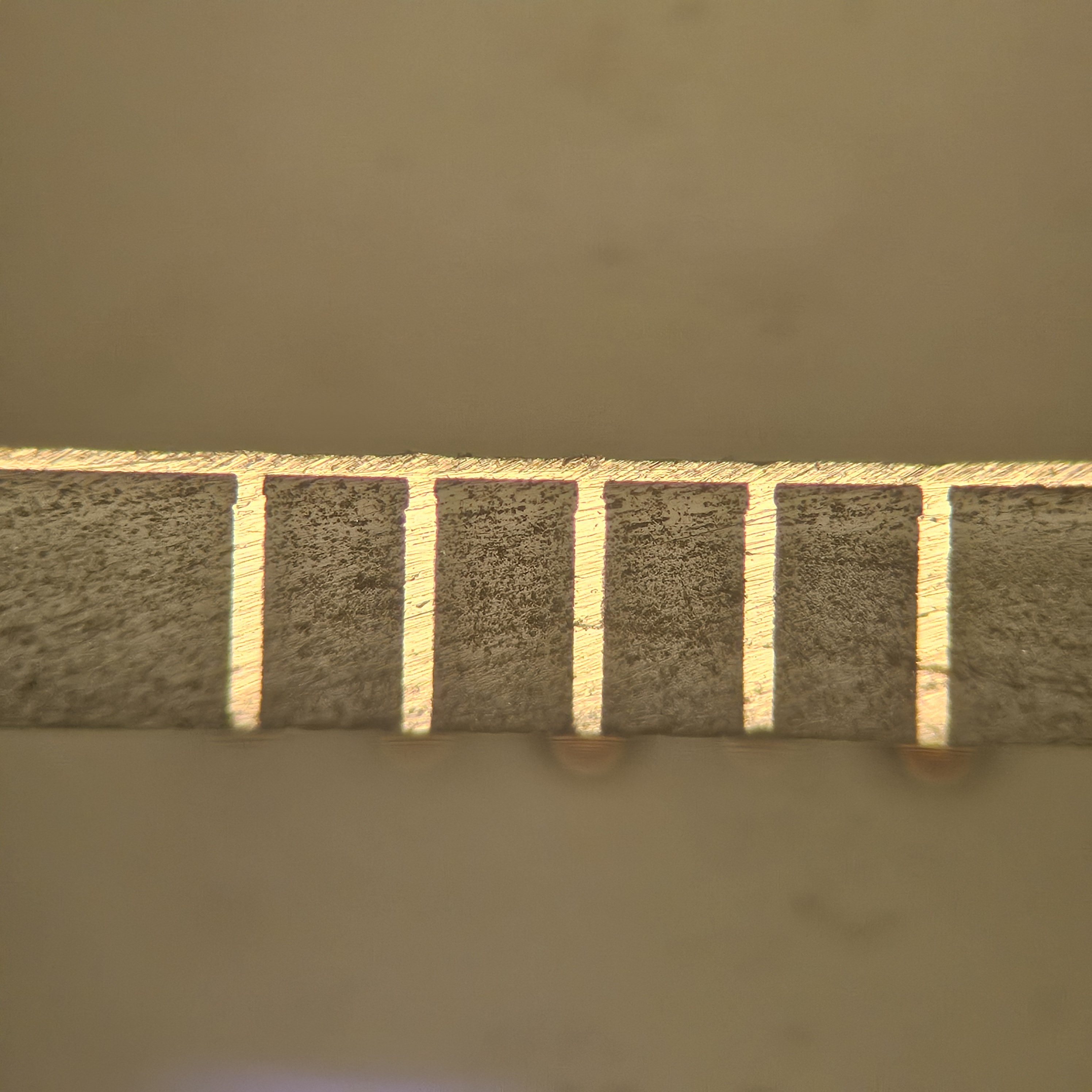
Unless the interposer is single sided, which can be the case, interposers have via made through the interposer to connect the faces. This is not the only function for via. Via can also be used for heat redistribution.
Here is a cross section of a glass wafer with copper filled via.
Interposer integration in PCB Electronics Assembly
The function of an interposer cannot replace all the systems function of the PCB which still needs to make connection to the external physical environment. The usual method to integrate an interposer into a PCB assembly is via a Ball Grid Array of solder connections. The necessary connections are usually on the bottom surface of the interposer via the usual set of solder balls.
Explore This Design Flow
Projects Using This Design Flow

Comments
Low Swing Signaling for Emerging Interposers
An interesting paper on 'Energy Efficiency of Low Swing Signaling for Emerging Interposer Technologies' from the University of Manchester. Energy efficiency of interposer-based interconnects depends highly on the total capacitance of the driven load as well as the interconnect length. When electrostatic discharge (ESD) protection is required, low swing signaling is superior in energy consumption due to the high capacitive load of the ESD circuit. The energy efficiency of low swing signaling increases in the case where large wire width in combination with low spacing are required.
Click to add new comment
To post a comment on this article, please log in to your account. New users can create an account.