SRAM Chiplet to minimise tape out costs for prototype systems. On-chip SRAM in ASICs can use a significant area, which equates to a significant cost. Using reusable off chip SRAM can save cost at the expense of system performance.
This SoC Labs project explores the use of Arm IP to create an SRAM chiplet design. Memory chiplets can be fabricated at lower cost and used across multiple projects.
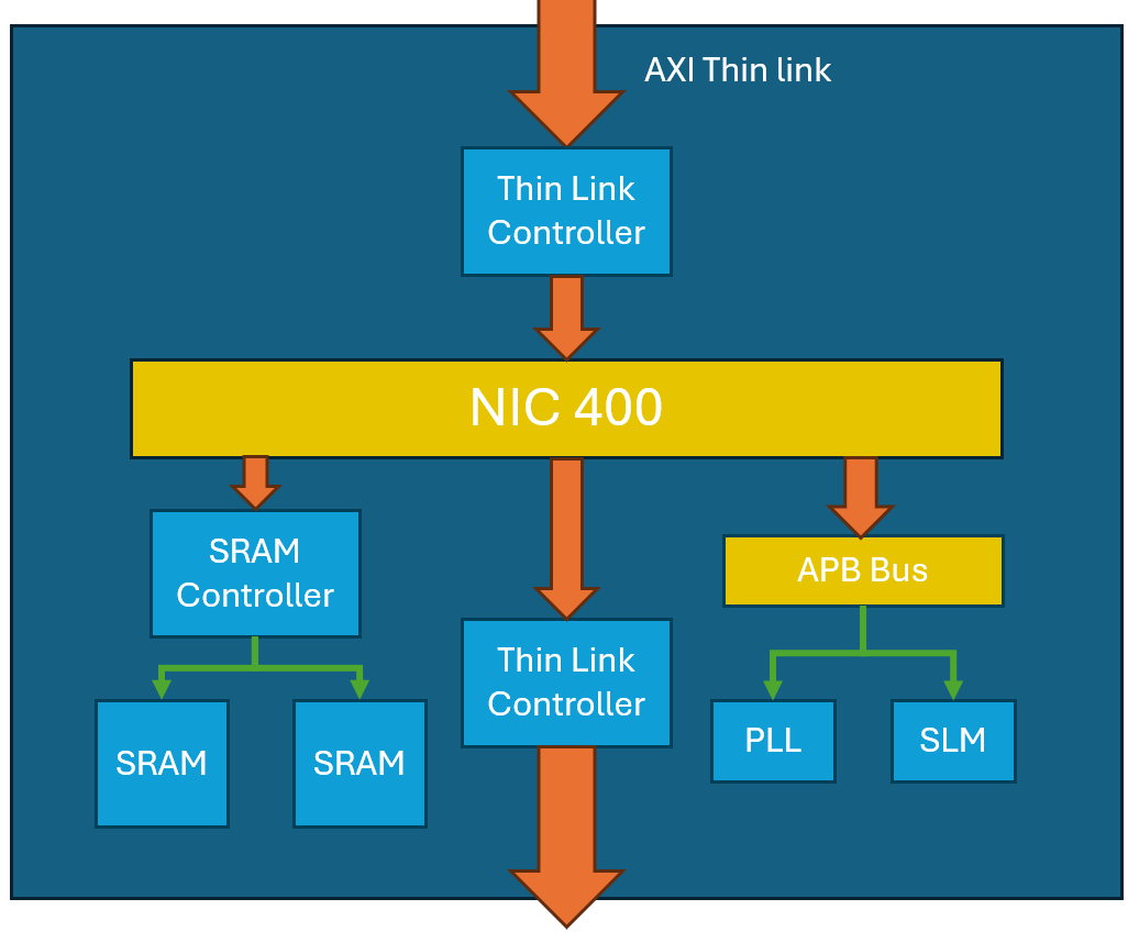
The use of a full AXI interface for external communication from a chip is expensive in terms of pin count and die area. Arm's Thin Links Protocol reduces the number of physical wires needed for connections by packing the AXI bus onto narrower data paths.
The architectural design of the SRAM Chiplet allows the use a daisy chain structure to create larger addressable memory regions by combining several SRAM chiplets. These could be arranged on an interposer to create a single System on Chip design made of multiple chiplets.
Explore This Design Common

Click to add new comment
To post a comment on this article, please log in to your account. New users can create an account.