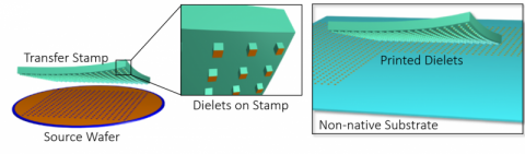
Micro-Transfer Printing enables the transfer of semiconductor parts fabricated in one material system including GaAs, InP, GaN, etc. to be attached to substrate in another material system with high precision and accuracy. The semiconductor parts are fabricated using their normal material system method. An additional etch process is implemented to create a release mechanism for the devices to come away from their native substrate. A variety of release layers have been developed. There is often a small remaining anchor/tether structure that breaks when the devices are lifted in the Micro-Transfer Printing process. The parts are lifted in parallel from the source wafer by a reusable, viscoelastic elastomer stamp that is designed to dimensions and tolerances to the parts to be processed. The parts are then printed / stamped onto the target substrate with alignment accuracy of about 1 micron dependent on the specific tool.

Click to add new comment
To post a comment on this article, please log in to your account. New users can create an account.