Chapter 9 covers the packaging of photonics based systems. Photonics systems are fundamental to data transmission and have been used for the generation of data through optical-based sensors, there is also a field of research in photonics for processing of data. Photonics systems are key enabler to continue the benefits that have been provided by Moore’s Law scaling of CMOS electronics in decrease in cost per function.
The packaging of photonic integrated circuits (PICs) will face the same challenges faced in packaging electronic ICs, with the added complexity of integrating both active and passive photonic elements as well as the necessary electronics.
PICs are used for many applications from LEDs, Lasers, Modulators, Plasmonics, Quantum Dots, Organic Photonics and Optical sensors, and from LiDAR to high bit rate Wavelength Division Multiplexing (WDM). The wide range of materials used requires unique thermal, electrical and mechanical solutions in the system integration (packaging) process and equipment. Key challenges to be addressed are:
- Physical density of bandwidth: To increase bandwidth using WMD, many applications will have to migrate from multimode to single mode fibers. This present cost and interconnection challenges.
- Interconnect for single-mode optical fiber: Low loss connection from the single mode fiber (about 8 microns) to substrate or on-chip systems will require different interconnect solutions.
- Thermal Drift of photonic components: Maintaining the wavelength stability is essential. Wavelength drift limits the number of channels in the WDM. The solutions today place demands on power consumption. New solutions with less temperature dependence will be required.
- Testing: This involves both photonic and electronic testing at the wafer, package and system levels. Access to test points within a complex 3D integrated electronic chips is challenging. It will be even more difficult where photonic test at each level is required.
New solutions to address current challenges are needed in the next 15 years. The solutions could be achieved through heterogenous integration approaches such as wafer-level packaging, 3D integration and integration of new materials.
Interconnect
While Photonics potentially offers the highest bandwidth density and lowest power requirement for moving data., challenges remain incorporating photonics into a system with non-photonic parts. There are power and area costs associated with Electrical-to-Optical (E-to-O) and Optical-to-Electrical (O-to-E) conversion that limits benefits for photonics when the distances are as short as in on-chip connections. There is also the consideration that components for integrated photonics are relatively large ~2µm while transistors are moving to single digit nm. 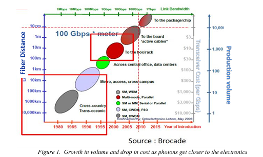
The Heterogeneous Integration of Photonics is looking to bring the optoelectronics interconnect to the package level and eventually to integrated circuits within the system. One of the challenges is that the costs of the transceivers need to reduce to produce the necessary decrease in cost per function compared to electronic transmission.
Substantial device miniaturization and improved energy efficiency of optoelectronic transceivers is required. Potential solutions to include on-chip photonics for electronic ICs are known and will be addressed.
Further out in the roadmap, for data processing the footprint associated with photonics devices, when normalized to their functionality, leaves room for substantial improvement, when compared to the footprint associated with electronic devices.
Substrates and Interposer development
HI is already combining PIC chips with existing electronic parts. Integration of photonic components into a sub-system or system may require accommodation of diverse materials including Si, InP, GaAs, and SiN with differences in fracture toughness and CTE. Many of the challenges are similar to those addressed in other forms of on-chip integration such as use of interposers, low cost interconnects, substrates and crosstalk. The current dominant package substrates used include organic laminates, Low temperature co-fired ceramics (LTCC), Glass and Si. Each substrate has design considerations including, differential CTE with semiconductor dies, mechanical stability, thermal conductivity, wiring density, I/O pitch and cost. Through Glass Vias (TGVs) and Through Silicon Vias (TSVs) are being actively developed for interposers for chip integration. Silicon has the advantage of being able to embed optical waveguides into the silicon substrate for heterogeneous integration of photonics, electronics and plasmonics.
Design tools
Design tools for silicon photonics are available.
AIM Photonics announced a Process Design Kit and multi-project wafer available in October of 2018. They also announced the addition of laser and CMOS integration with a silicon interposer.
Main Applications for Photonics
The global network: The 3D integration in System in Package (SiP) architecture will lead to lower power, high bandwidth, smaller size and higher logic performance. For example, a 3D SIP microserver with 70X can be achieved and adding a photonic layer will further reduce power and latency. The integration of PICs and Electronic ICs are of major interest to future server and high performance computer systems.
Photonics in Data Centers: As of 2021, 100 Gb/s is the dominant data rate used in hysperscale data centers and expected to increase to 200 Gb/s, 400 Gb/s increasing to even 1.6 Tb/s. Integration of photonics and electronics in the co-packaged optical system is the solution being pursued. For example Intel demonstrated a 12.8Tb/s co-packaged optical switch in Feb 2020. This integration approach is compatible with the scaling plans for data center roadmap.
Photonics in automotive: Today's automotive industry has incorporated a range of photonics systems including internal communication networks, infotainment applications, LiDAR, Cameras and Infrared sensors. In the Media Oriented Systems Transport, the use of photonics offers superior data rates, bandwidth, reliability and robustness compared to electronic solutions. The automotive industry is relying on light/image or optical sensors for a wide range of safety technologies for occupant safety, intruder detection, lane departure warning and blind spot detection. In addition the emergence of autonomous vehicle will incorporate LiDAR systems.

Comments
UCIe based optical interconnect chiplet
Ayar Labs have announced a Universal Chiplet Interconnect Express™ (UCIe™) based 8 Tbps bandwidth optical interconnect chiplet. The TeraPHY™ optical I/O chiplet combines silicon photonics with CMOS manufactured parts within a multi-chip package. Ayar Labs believe compatibility with the UCIe standard will allow their optical interconnect technology to be interoperable with chiplets from different vendors and ease the design and integration work for their customer's designs.
Video on Ayar Labs
If you prefer to watch a video of the Ayar Labs offering then see here.
Click to add new comment
To post a comment on this article, please log in to your account. New users can create an account.