The cost of Electrostatic Discharge (ESD) in damaged electronic devices is estimated to be in Billions of Dollars. The loss increases as the complexity of the system grows. As heterogeneous integration (HI) systems grow in complexity there is work within the industry to establish standards, design practice and manufacturing controls to limit loses.
Before getting into details it is worth noting that the community of engineers focused on Electrostatic Discharge is like a well connected HI system. Take the EOS/ESD Association (ESDA), it is accredited by the American National Standards Institute (ANSI) to write and produce standards on electrostatics and also represents the United States at the International Electrotechnical Commission (IEC) in the area of electrostatics. The Industry Council on ESD Target Levels is not affiliated to any standards body but is an industry body that makes recommendations for next generation qualification target levels for human body model (HBM) and charged device model (CDM), in accordance with the ESDA Technology Roadmap, while also taking into account both state-of-the-art IC design and manufacturing constraints. JEDEC also create standards that focus on the semiconductor industry. These standards can be closely related for example JEDEC JESD625B (January 2012) and ANSI/ESD S20.20-2014.
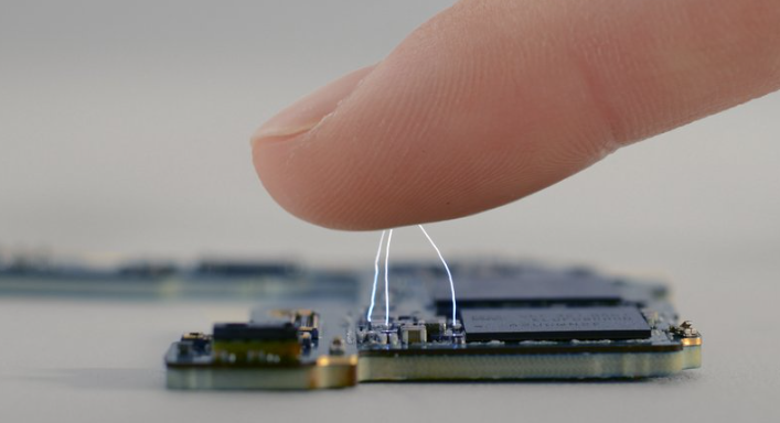
Die-to-Die (D2D) interfaces are a critical connection point for a heterogeneous integration systems. In order to protect the internal circuits of a die against electrostatic discharge (ESD) stresses, on-chip ESD protection circuits are used at die interfaces. These protection circuits have an impact on the signal interfaces especially for high speed I/O and RF signals. The industry faces a careful balance between CDM robustness and performance of HI systems. The Council has demonstrated that there is safe margin to allow ESD levels to be reduced for the CDM roadmap for die-to-die (D2D) interfaces.
The early work of the council looked to develop a system level ESD protection design strategy as there was an over reliance by system designers on IC component protection. The "System-Efficient ESD Design" (SEED) looks at system level ESD robustness which is affected by all components and their interactions. The design and tests for ESD undertaken by IC component providers are based on actions on the pins of an unpowered part in isolation. They are aimed to allow the IC to survive the various manufacturing steps based on being in a controlled ESD environment. Using components with good ESD protection does not mean a system made from them is well protected. By contract the design and tests for a system are based on expected actions in a system's normal powered operation with System level ESD robustness affected by all components and their interactions. Stress is applied between specific locations on the system and the power supply reference ground. Discharge paths, associated currents and wave shapes will be different for these different stress methods. Designers should not simply depend on large area on-chip protection as a good strategy for robust system ESD design.
The Council recommendation on Implementation of Effective ESD Robust Designs introduces new system diagnosis methods, a “cost vs. performance vs. robustness” model for prevention of system level ESD failure and a technology roadmap that highlights challenges for system ESD design improvement. One of the key aims of the Council is to improve communication and coordination between system designers and IC providers, this is very similar to the aim of the CHIMES IKC in bringing together the disparate parts of the UK electronics systems community.
Another aim is to develop a methodology to assess the ESD implications for the entire system using simulation data but recognises a full design flow will only be achieved through a common effort across the whole electronic industry. A framework for such modeling has been defined through IEC 61433-6, but work is needed on simulation programs with integrated circuit emphasis (SPICE) models to be enhanced to describe component behavior in the ESD range such that they can be included in the standard design flow for electronic systems. Standardisation activities involving the EDA tool vendors, component suppliers and system design community must continue.
There has been an over dependency on the IC design and test for protection and that responsibility is expected to gradually shift more towards being a system design expertise. In the current climate of incomplete ESD data and design tool support for the systems designer there is a tendency to stick to already well known designs options and less willingness to consider better options for improved product function or margin improving cost reductions. What is needed is a reliable methodology to design and qualify the ESD performance of specific systems by the system designer to enable them to make better design choices.

Click to add new comment
To post a comment on this article, please log in to your account. New users can create an account.