Cap Gemini have produced an interesting report on the semiconductor ecosystem and the down-stream industries that depend on it.
In terms of demand for semiconductors, the down-stream industries such as automotive, telecoms, aerospace and defense, medical, industrial equipment, financial, energy, etc. see double the demand for semiconductors as the semiconductor industry. A growing number are concerned over the ability of the industry to supply their needs.
The current driver of cloud based Artificial Intelligence is largest demand but edge based devices, wearables and augmented/virtual reality are not far behind in expected demand. The cloud AI demand focuses on semiconductors for memory and parallel compute (GPUs, NPUs, ...) but there is also strong demand for custom ASIC to allow companies to differentiate themselves from the current dominate players as well as strong growth in power devices and MEMS/sensors.
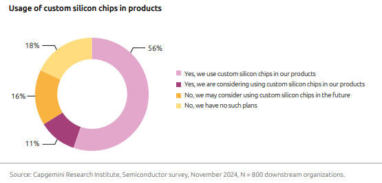
There is a growing interest within companies in developing differentiation by leveraging custom chip designs. There are various drivers, protecting IP and data, cost, local market place specific demands, etc. There are also a number of issues restricting the development of a broader market in custom ASIC including , effort to develop a complex design in-house, acquiring talent, cost of cutting-edge design tools, and testing costs.
In part this has been driven by the industry trend to bring together more and more function into single chip System on Chip solutions. This makes the task of the overall electronic system design task simpler, if more of the function of the system is delivered by an off the shelf part, but harder to differentiate unless the System on Chip function in the single die is replicated. A new SoC implementation does not usually change all the functions, just some, yet the whole SoC design has to be reverified, usually at a very high cost.
The question for the IKC is 'are we at an inflection point?'. Will the concepts of System on Chip disaggregation, 'chiplets' and heterogenous integration lead to a lower cost model for creating custom electronic systems. Will IP design houses move from selling IP to selling 'chiplets', will a chiplet (bare die) and interposer market place develop in a similar way to the current packaged electronic component and Printed Circuit Board market develop. If if does then potentially many more companies will develop custom semiconductor parts using third party foundry services.
The most advanced technology nodes are not scaling in terms of reducing cost. Fabricating some parts of a System on Chip on an advanced node gives no benefit apart from the function being in a single die. If the interconnect of the interposer can work at a high enough rate then compiling a system from a collection of die at varying semiconductor processes can be a way to overcome the cost challenges of adopting custom silicon to differentiate the total electronic system.
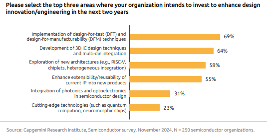
The report identifies some trends from the semiconductor industry. The development of 3D IC techniques and multi-die integration is one of the top areas of focus for investment and that organizations will prioritize the development of 3D IC design techniques and multi-die integration in the next two years. It is also interesting that the top item 'design-for-test' and the forth item, 're-use of IP in new products' are in my view the same driver. If IP can be packaged in re-usable and smaller chips that require less effort each to verify and that these can be brought together into systems as chiplets at a reduced cost than a new monolithic System on Chip design then it will be an inflection point in the industry.
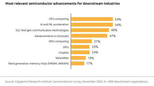
The companies downstream of the semiconductor industry, such as automotive, telecoms, aerospace and defense, etc. will always lag a little but they also indicate that after there immediate focus of more compute for AI workloads and associated data movement, that chiplets is the next most relevant advancement.
These are the challenges the IKC faces and has been established to work towards. To work with the UK electronic systems community, those down stream of the core semiconductor industry, to help them understand the benefits of the 'chiplets' and heterogenous integration of them. Some survey work undertaken with IMAPS UK as part of the InterposeUK project split the UK community into three rough groups, those that felt the need for heterogenous integration and advanced packaging was here today, those that felt it was within their 3 year horizon and those who are not yet seeing demand for it.
This to me indicates that the semiconductor industry is likely to move from an early adopter market to an early majority market in the next 2-3 years and that leading edge down stream companies will follow. The IKC has the task of ensuring the UK does not fall behind the curve, remains competitive and shows a clear path for the UK early majority market to develop.

Click to add new comment
To post a comment on this article, please log in to your account. New users can create an account.